Check out our latest products
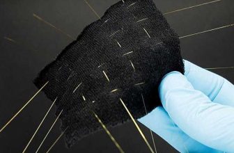
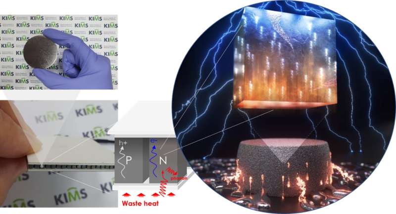
A research team at Korea Institute of Materials Science has developed a novel n-type thermoelectric semiconductor material, advancing the ability to recycle waste heat from industrial sectors.

The innovative thermoelectric material, based on bismuth telluride (Bi-Te) with atomic-scale defects, improves the efficiency of thermoelectric power generators. These generators convert waste heat below 200℃ from sources like factories, automobiles, and ships into electrical energy. Thermoelectric devices are made up of p-type and n-type semiconductors, which use temperature differences to generate power.
While significant progress had been made in enhancing p-type thermoelectric materials, improving n-type semiconductors had been a longstanding challenge. The difficulty in controlling the composition and microstructure of n-type materials, which contain selenium (Se), has hindered the commercialization of thermoelectric technology. However, this research team has now overcome these limitations by focusing on the critical role of n-type materials in determining the performance of thermoelectric power generators.

This thermoelectric material holds immense potential for industries seeking to reduce energy waste and enhance efficiency. Manufacturers in the automotive, shipbuilding, and heavy industries could particularly benefit from incorporating this technology into their processes, as it targets waste heat recovery. Furthermore, its compact design may also find applications in consumer electronics, offering a way to harness body heat and other low-level thermal sources.
The key to this research lies in the doping process and material selection. Doping materials enhance the electrical conductivity of semiconductors. The team opted to replace selenium (Se) with antimony (Sb) in n-type bismuth telluride, a strategy that had proven effective in p-type materials. This adjustment significantly enhanced the electrical properties of the n-type semiconductor.
In addition, the team developed a technique to induce “atomic defects,” which increase electron formation, and “dislocation networks” that reduce thermal conductivity by scattering lattice phonons. Using powder metallurgy, they produced thermoelectric materials that double the electrical conductivity while lowering thermal conductivity. This method allows for the easy fabrication of materials into desired shapes and sizes.
Dr. Kyung Tae Kim, Department of 3D Printing Materials, Korea Institute of Materials Science, Republic of Korea, remarked, “This study has laid a stepping stone to solving the property control of n-type thermoelectric semiconductors, which has been an obstacle to recycling various types of waste heat below 200℃.”
The global thermoelectric market is expected to grow rapidly, reaching $1.18 billion by 2029.


![[5G & 2.4G] Indoor/Outdoor Security Camera for Home, Baby/Elder/Dog/Pet Camera with Phone App, Wi-Fi Camera w/Spotlight, Color Night Vision, 2-Way Audio, 24/7, SD/Cloud Storage, Work w/Alexa, 2Pack](https://m.media-amazon.com/images/I/71gzKbvCrrL._AC_SL1500_.jpg)


![[3 Pack] Sport Bands Compatible with Fitbit Charge 5 Bands Women Men, Adjustable Soft Silicone Charge 5 Wristband Strap for Fitbit Charge 5, Large](https://m.media-amazon.com/images/I/61Tqj4Sz2rL._AC_SL1500_.jpg)


