Check out our latest products
On Dec. 9, IBM unveiled a breakthrough in co-packaging optics that could reduce GPU downtime and accelerate AI training.
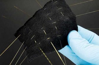
IBM’s working prototype significantly increases the number of optical fibers connecting at the edge of a silicon photonics chip by replacing traditional glass with a polymer optical waveguide. This innovative approach could pave the way for faster, more efficient data transfer and allow data centers to handle greater workloads.
The idea of co-packaged optics has been around for a long time, but IBM’s process enables what the company calls the world’s first stress-tested prototype.
IBM spokespeople didn’t directly address questions about availability or a timeline. Instead, they emphasized their intent to develop a roadmap and expressed their openness to sharing design material with foundries in the future.
“At the end, the chip product companies will have to ask for that, and then the product companies will design that into their chip design, and the foundries can manufacture,” Makesh Khare, general manager of IBM semiconductors, said at a briefing. “But it has no special requirement regarding the foundry aspect. It will have a design aspect we can provide to the chip companies.”
What makes a polymer optical waveguide stand out?
Co-packaged optics with polymer optical waveguides are an alternative to copper connections and are often used to link GPU accelerators in data centers. These sit at the edge of a chip and let many high-density bundles of optical fibers squeeze into a tiny space, with half a micron or less between the fiber and the connector. IBM said this brings a dramatic bandwidth boost between chips compared to electrical connections.
The size — a 50-micron pitch — also differentiates the prototype. 250-micron pitch is a standard size. Going smaller translates to increased bandwidth.
The polymer optical waveguide stacks in up to four layers for up to 128 channels. At the “beachfront” where the connector meets the chip, it presents 51 fibers per millimeter.
“The big deal is not only that we’ve got this big density enhancement for communications on module, but we’ve also demonstrated that this is compatible with stress tests that optical links haven’t been passing in the past,” John Knickerbocker, distinguished engineer at IBM research, said in a press release.
“This co-packaged optics innovation is basically bringing the power of fiber optics on the chip itself,” Khare added.
IBM’s polymer optical waveguide may compete with novel connectivity processes like the Ranovus Odin electronic and photonic integrated circuit or linear-drive pluggable optics. Researchers are also experimenting with glass ribbons or vertical-graded interconnections in this area.
Knickerbocker said in the briefing: “It’s hard to say who is up in front“ between polymer optical waveguides and linear-drive pluggable optics.
IBM has manufactured co-packaged optics with polymer optical waveguides at its Bromont testing facility in Quebec.
SEE: Data centers will need more power for AI training as hyperscalers offer more advanced models.
The proposed market: Data centers used to train AI
IBM proposes the new connector could benefit the booming generative AI industry by:
- Power draw reduction (of up to 5 times) mid-range electrical interconnects, including at long ranges (hundreds of meters).
- Reduction in the time it takes to train a large language model, from three months to three weeks.
- Increased energy efficiency.
“With this breakthrough, tomorrow’s chips will communicate much like how fiber optics cables carry data in and out of data centers, ushering in a new era of faster, more sustainable communications that can handle the AI workloads of the future,” SVP and Director of Research Dario Gil said in a press release.


![[5G & 2.4G] Indoor/Outdoor Security Camera for Home, Baby/Elder/Dog/Pet Camera with Phone App, Wi-Fi Camera w/Spotlight, Color Night Vision, 2-Way Audio, 24/7, SD/Cloud Storage, Work w/Alexa, 2Pack](https://m.media-amazon.com/images/I/71gzKbvCrrL._AC_SL1500_.jpg)


![[3 Pack] Sport Bands Compatible with Fitbit Charge 5 Bands Women Men, Adjustable Soft Silicone Charge 5 Wristband Strap for Fitbit Charge 5, Large](https://m.media-amazon.com/images/I/61Tqj4Sz2rL._AC_SL1500_.jpg)


