Printed Circuit Board Design Engineer At Aether Semiconductors In Sahibzada Ajit Singh Nagar

Check out our latest products

![[5G & 2.4G] Indoor/Outdoor Security Camera for Home, Baby/Elder/Dog/Pet Camera with Phone App, Wi-Fi Camera w/Spotlight, Color Night Vision, 2-Way Audio, 24/7, SD/Cloud Storage, Work w/Alexa, 2Pack](https://m.media-amazon.com/images/I/71gzKbvCrrL._AC_SL1500_.jpg)


– Advertisement –
Location: Sahibzada Ajit Singh Nagar
Company: Aether Semiconductors
Experience Level: 1 – 8 years
– Advertisement –

Communication: Good command over English
Mail Id: [email protected]
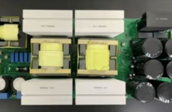
Job Responsibilities for PCB Design Engineer (4-6 Years of Experience) in Semiconductor Equipment Engineering:
PCB Design and Development:
- Design and develop Printed Circuit Boards (PCBs) for semiconductor equipment with a focus on high-power systems, controllers, and embedded applications.
- Perform schematic capture and layout design for multi-layer and high-density boards using tools such as Altium Designer, OrCAD, or similar software.
- Ensure compliance with design for manufacturability (DFM), design for testing (DFT), and signal integrity guidelines.
High-Power and Embedded Systems Integration:
- Develop PCBs that incorporate power management, high-power circuits, and advanced embedded controllers.
- Work on integrating microcontrollers, programmable logic devices (PLDs), and FPGAs into board designs for semiconductor equipment.
- Troubleshoot and optimize boards for thermal management, noise reduction, and high reliability under operational conditions.
Collaboration and Testing:
- Collaborate with cross-functional teams, including mechanical, software, and system engineers, to ensure successful product integration.
- Conduct board bring-up, functional testing, and debugging of PCBs to ensure performance meets specifications.
- Analyze and resolve hardware issues related to semiconductor equipment functionality and performance.
Technical Documentation:
- Create and maintain comprehensive design documentation, including schematics, layouts, BOMs, and test procedures.
- Support the preparation of technical reports and documentation for internal teams and stakeholders.
Continuous Improvement:
- Stay updated on the latest advancements in PCB design, semiconductor technology, and embedded systems.
- Identify opportunities to enhance design processes, improve product performance, and optimize cost.
Compliance and Standards:
- Ensure designs meet industry standards, including IPC guidelines, EMI/EMC requirements, and safety certifications.
- Perform validation and verification to align with semiconductor equipment engineering standards.
Required Skills & Qualifications
- Education: A bachelor’s degree in Electrical Engineering or an M.Tech in Electronics Engineering, or a related field.
- Experience: 2-6 years of PCB design experience in the semiconductor industry or related fields.
- Technical Proficiency: Proficiency in PCB design tools such as Altium Designer and Cadence Allegro, with a solid understanding of IPC standards and experience in high-speed, high-density PCB designs.
- Simulation Skills: Expertise in simulation tools for signal integrity and thermal management, including software like ANSYS and HyperLynx.
- Analytical Skills: Strong problem-solving capabilities with hands-on experience in testing and troubleshooting PCB designs.
- Attention to Detail: Exceptional accuracy and detail orientation in design processes and documentation.
- Communication Skills: Excellent ability to convey design concepts and findings effectively to both technical and non-technical stakeholders.
Basic Requirement
- The candidate must be willing to relocate to the Mohali location. Preference will be given to candidates with an immediate or one-month notice period. Additionally, priority will be given to those with extensive experience in the semiconductor industry.

![[3 Pack] Sport Bands Compatible with Fitbit Charge 5 Bands Women Men, Adjustable Soft Silicone Charge 5 Wristband Strap for Fitbit Charge 5, Large](https://m.media-amazon.com/images/I/61Tqj4Sz2rL._AC_SL1500_.jpg)