Check out our latest products
Evolving with 3D AOI and smart factory standards, PCB inspection today is all about absolute precision, efficiency, and reliability. How does the global standard keep pace as Industry 4.0-driven automation continues to ensure high-quality manufacturing?
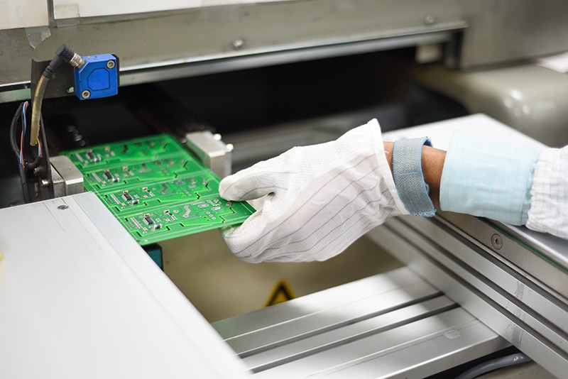
In recent years, printed circuit board (PCB) inspection has undergone a remarkable transition, largely driven by innovations like 3D automated optical inspection (AOI) tools. But first of all, what exactly is AOI? Widely used in the electronics manufacturing industry, it is a visual inspection technology to enhance product quality by efficiently identifying defects during the manufacturing process.
AOI combines advanced optics, cameras, and image processing capabilities for scrutiny. A camera autonomously scans the device under test for both catastrophic failure (such as missing components) and quality defects (like fillet shape or component skew).

These technologies have revolutionised the way quality control is handled, improving the efficiency, precision, and scalability of PCB manufacturing, pinpointing surface and soldering defects. Unlike 2D AOI, which relies on two-dimensional images, 3D AOI creates a detailed board profile using various imaging technologies. It captures the height, volume, and shape of solder joints and components, allowing for a more accurate analysis.
How the power of 3D AOI works
3D AOI adds another level to PCB inspection by accurately detecting defects like solder joint issues, component presence or absence, and lead coplanarity. It reduces false positives by analysing depth and volume, which helps minimise errors caused by lighting or color variations. Additionally, its ability to inspect intricate details such as solder paste height and component orientation, ensures a comprehensive examination, making it ideal for high-density PCBs.
The architecture of AOI for PCB testing
The main components of 3D AOI include multiple high-resolution cameras, advanced lighting, and structured light projectors. The cameras capture images from different angles, while structured light projectors emit light patterns onto the PCB surface. These patterns are distorted based on the height and contours of the components and solder joints, allowing the system to generate a 3D topographical model of the board.
Another critical component is sophisticated image processing software that analyses the 3D data to detect defects. The software can compare the scanned 3D model with predefined CAD data or golden board standards to identify any anomalies. Additionally, machine learning algorithms and data analytics can be integrated to improve detection accuracy and efficiency over time.
What can render a PCB defective? The answer is, the IPC-A-610…
The IPC-A-610 standard is the global benchmark set by the Institute for Printed Circuits (IPC) for the acceptability of electronic assemblies, providing essential criteria for soldering quality, component placement and alignment, and overall workmanship in PCB assemblies.
The standard outlines criteria for acceptable solder joint specifications, including fillet size and shape, ensuring top-quality standards. It also provides detailed guidelines for lighting and magnification during inspections, with most conducted at magnifications under 20X, and 40X considered the ‘referee’ magnification. However, higher magnifications are limited by the depth of field of optical imaging.
Another critical aspect of IPC-A-610 involves the placement of solder balls. If solder balls are located within 0.13mm of traces, they violate the minimum electrical clearance principle and can compromise the electrical reliability of the assembled PCB. A PCB is deemed defective if there are five solder balls (<=0.13mm) within 600mm².
It also addresses issues like component skew, coplanarity, and orientation, all of which impact the long-term reliability of electronic assemblies.
A spotlight on IPC-CFX and IPC-HERMS-9852
As the manufacturing sector embraces Industry 4.0, smart factory standards like IPC-CFX (connected factory exchange) and IPC-HERMES-9852 play a crucial role in ensuring the seamless integration of inspection systems into automated production lines.
IPC-CFX
It is an industry-developed, open international standard forming the backbone of Factory of the Future applications. It provides a plug-and-play solution that simplifies and standardises machine-to-machine communication while enabling efficient machine-to-business and business-to-machine interactions.
IPC-HERMES-9852
A successor to the Surface Mount Equipment Manufacturers Association (SMEMA) standard, officially known as IPC-SMEMA-9851, IPC-HERMES-9852 introduces several improvements, including:
- Simplified wiring: uses Ethernet instead of complex physical wiring
- Modern data transmission: supports widely used formats like TCP/IP and XML
- Optimised barcode scanning: reduces the number of required barcode scanners to one at the start of the production line
- Enhanced data transmission: allows downstream machines to receive board data, such as barcodes and dimensions
By the end of 2018, IPC officially recognised the Hermes Standard as the successor to IPC-SMEMA-9851, the globally accepted standard for machine-to-machine communication in SMT (surface mount technology) for PCB handover.
Accordingly, the Hermes Standard was assigned an IPC designation and is now called IPC-HERMES-9852. The latest versions, 1.5 and 1.2, not only replace the electrical SMEMA interface but also expand its functionality. They facilitate the transmission of essential data, including unique board identifiers, the equipment ID of the first machine detecting a PCB, barcodes, conveyor speed, and specific product type information.
This standard is designed to harmonise equipment communication and control in smart factories, ensuring the smooth integration of inspection systems such as AOI machines into fully automated environments.
Final Thoughts
The integration of 3D AOI and smart factory standards empowers PCB manufacturers to meet rising demands for precision and reliability. For a company investing in a 3D AOI system, it is about ensuring top-tier quality and guaranteeing the longevity of their electronic products!
References
- www.eaconnect.com
- www.elmetlabs.com
- www.7pcb.com
- wikepedia.org
- www.ipc.org


![[5G & 2.4G] Indoor/Outdoor Security Camera for Home, Baby/Elder/Dog/Pet Camera with Phone App, Wi-Fi Camera w/Spotlight, Color Night Vision, 2-Way Audio, 24/7, SD/Cloud Storage, Work w/Alexa, 2Pack](https://m.media-amazon.com/images/I/71gzKbvCrrL._AC_SL1500_.jpg)


![[3 Pack] Sport Bands Compatible with Fitbit Charge 5 Bands Women Men, Adjustable Soft Silicone Charge 5 Wristband Strap for Fitbit Charge 5, Large](https://m.media-amazon.com/images/I/61Tqj4Sz2rL._AC_SL1500_.jpg)


