
Check out our latest products

![[5G & 2.4G] Indoor/Outdoor Security Camera for Home, Baby/Elder/Dog/Pet Camera with Phone App, Wi-Fi Camera w/Spotlight, Color Night Vision, 2-Way Audio, 24/7, SD/Cloud Storage, Work w/Alexa, 2Pack](https://m.media-amazon.com/images/I/71gzKbvCrrL._AC_SL1500_.jpg)


Scientists in South Korea have developed a conductive-bridge interlayer contact, overcoming efficiency limitations in 2D semiconductor-based photodiodes.
Photodiodes, key components in photovoltaics, sensors, imaging, and communication technologies, convert light into electrical current. Researchers have been striving to enhance their efficiency, with a growing focus on two-dimensional (2D) semiconductors—materials only a few atomic layers thick that offer unique electrical properties.
However, 2D semiconductor-based photodiodes have struggled to meet performance expectations due to Fermi level pinning, a phenomenon that disrupts charge flow at metal-semiconductor interfaces. To tackle this challenge, a team from the Korea Institute of Science and Technology (KIST), Korea University, and Yonsei University has designed an innovative conductive-bridge interlayer contact. Their research, published in Nature Electronics, could mark a turning point for optoelectronic advancements.

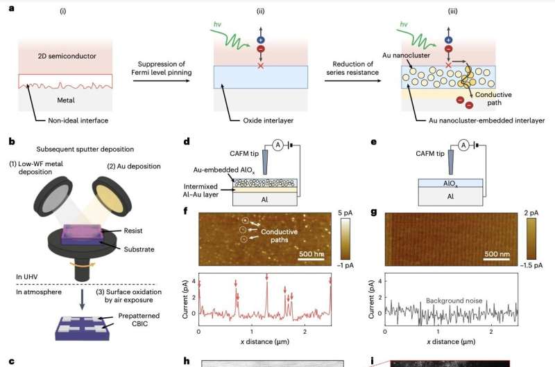
“Photodiodes based on two-dimensional semiconductors have great potential, but their photovoltaic efficiency is hindered by strong Fermi level pinning,” wrote Jisu Jang, Jung Pyo Hong, and their team. “Metal-interlayer-semiconductor contacts can mitigate this issue, but they often increase resistance. Our conductive-bridge interlayer contact provides both Fermi level depinning and low resistance.”
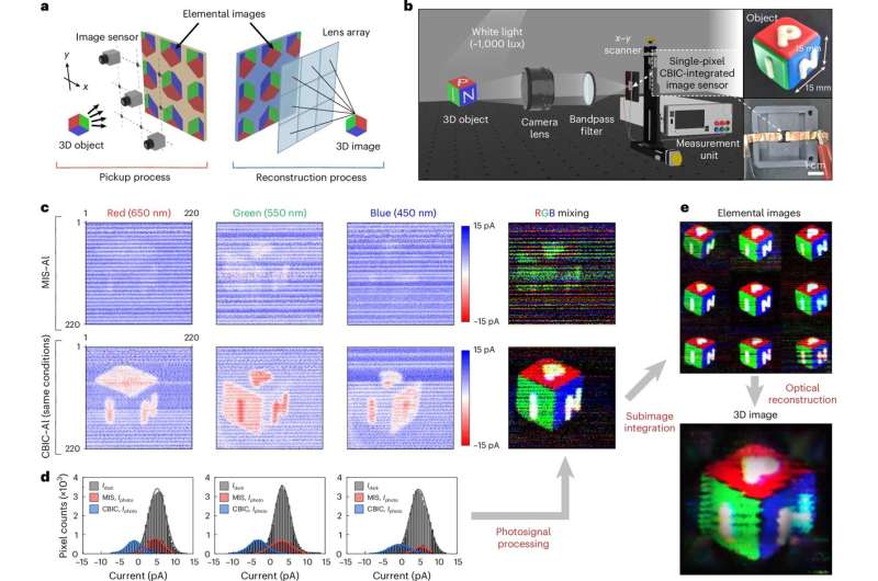
The team’s novel interlayer comprises an insulating oxide material embedded with gold nanoclusters. This structure isolates the metal from the 2D semiconductor while the gold nanoclusters create conductive paths, enhancing charge transport. Implementing this technology in a tungsten disulfide (WS₂) photodiode, they achieved a photoresponsivity of 0.29 A/W, a linear dynamic range of 122 dB, and a power conversion efficiency of 9.9%.
Beyond boosting efficiency, this approach allows for deeper exploration of photocarrier dynamics. The researchers also demonstrated its potential for full-color 2D and 3D imaging applications. Looking ahead, the conductive-bridge interlayer could be integrated into various 2D semiconductor-based optoelectronic devices, paving the way for advancements in imaging, sensing, and communication technologies.

![[3 Pack] Sport Bands Compatible with Fitbit Charge 5 Bands Women Men, Adjustable Soft Silicone Charge 5 Wristband Strap for Fitbit Charge 5, Large](https://m.media-amazon.com/images/I/61Tqj4Sz2rL._AC_SL1500_.jpg)