
Check out our latest products

![[5G & 2.4G] Indoor/Outdoor Security Camera for Home, Baby/Elder/Dog/Pet Camera with Phone App, Wi-Fi Camera w/Spotlight, Color Night Vision, 2-Way Audio, 24/7, SD/Cloud Storage, Work w/Alexa, 2Pack](https://m.media-amazon.com/images/I/71gzKbvCrrL._AC_SL1500_.jpg)


A frequency-dependent switch designed for PSpice simulation empowers experts to address challenges in advanced systems, seamlessly integrating into diverse electronic circuits.
Switches may be used in any device/circuit in UHF or higher radio bands that need to route signals through multiple paths. Switches in different configurations are used in ATE (automatic test equipment) systems. Solid state switches can be divided into two primary categories: mechanical, relay-operated, PIN diode and FETs. They can be used,
- to switch a single signal between double outputs,
- to connect different multiple outputs delivering signals to port connections in parallel,
- to route change (bypass) a voltage around rather than through a circuit element or system.
Design and modelling of a voltage/current-controlled analogue behavioural model switch compatible with PSpice circuit simulation software are described with examples in the frequency domain.
Simulation method
The PSpice method to obtain an equivalent circuit for different switches using analogue behavioural modelling is described. Other works in this field used different configurations using polynomial voltage/current source models of the original PSpice program.
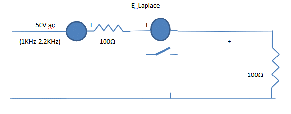
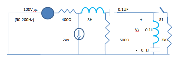
Table I describes (Fig: 1) the PSpice procedure to obtain frequency-dependence, which behaves as short at 1700Hz and becomes open circuit at other operating frequencies of Fig: 1 [equivalent to performing switching (on/off) action]. The E Laplace in Fig: 1 describes an on/off resistor using analogue behavioural modelling of PSpice with the Laplace option.

Table I. Frequency description of switch operation (Fig: 1)
| **** 10/03/23 16:43:29 ****** PSpice Lite (October 2012) ****** ID# 10813 **** |
| Frequency-dependent switch simulation |
| Circuit description |
| V2 1 0 AC 1 |
| R13 1 3 100 |
| E34 3 4 LAPLACE {I(E34)} = {(ABS(S)/(2.0*3.141592653589793)-1700)*1E8} |
| R40 4 0 100 |
| .AC LIN 13 1KHz 2.2KHz |
| .PRINT AC VM(1) VM(3) VM(4) |
| .OP |
| .end |
| **** 10/03/23 16:43:29 ****** PSpice Lite (October 2012) ****** ID# 10813 **** |
| Frequency-dependent switch simulation |
| Small signal bias solution Temperature = 27.000 DEG C |
| Node voltage |
| ( 1) 0.0000 ( 3) 0.0000 ( 4) 0.0000 |
| Voltage source currents |
| Name Current |
| V2 0.000E+00 |
| Total power dissipation 0.00E+00 watts |
| **** 10/03/23 16:43:29 ****** PSpice Lite (October 2012) ****** ID# 10813 **** |
| Frequency-dependent switch simulation |
| Operating point information Temperature = 27.000 DEG C |
| Voltage-controlled voltage sources |
| Name E34 |
| V-source 0.000E+00 |
| I-source 0.000E+00 |
| **** 10/03/23 16:43:29 ****** PSpice Lite (October 2012) ****** ID# 10813 **** |
| Frequency-dependent switch simulation |
| AC analysis Temperature = 27.000 DEG C |
| FREQ VM(1) VM(3) VM(4) |
| 1.000E+03 1.000E+00 1.000E+00 1.429E-09 |
| 1.100E+03 1.000E+00 1.000E+00 1.667E-09 |
| 1.200E+03 1.000E+00 1.000E+00 2.000E-09 |
| 1.300E+03 1.000E+00 1.000E+00 2.500E-09 |
| 1.400E+03 1.000E+00 1.000E+00 3.333E-09 |
| 1.500E+03 1.000E+00 1.000E+00 5.000E-09 |
| 1.600E+03 1.000E+00 1.000E+00 1.000E-08 |
| 1.700E+03 1.000E+00 5.007E-01 4.993E-01 |
| 1.800E+03 1.000E+00 1.000E+00 1.000E-08 |
| 1.900E+03 1.000E+00 1.000E+00 5.000E-09 |
| 2.000E+03 1.000E+00 1.000E+00 3.333E-09 |
| 2.100E+03 1.000E+00 1.000E+00 2.500E-09 |
| 2.200E+03 1.000E+00 1.000E+00 2.000E-09 |
It can be observed (Table I) that due to the switching action at 1.7KHz, all the voltage is transferred to the output node (4) from the node (3).
Table II. PSpice program description of switching (Fig:2)
| **** 10/03/23 16:33:07 ****** PSpice Lite (October 2012) ****** ID# 10813 **** |
| Frequency-dependent AC switch simulation |
| Circuit description |
| V2 1 0 AC 100 |
| R13 1 2 400 |
| G1 2 0 4 0 2 |
| L23 2 3 0.3 |
| R30 3 0 500 |
| C34 3 4 0.1UF |
| L46 4 6 0.1 |
| C60 6 0 0.1 |
| E45 4 5 LAPLACE {I(E45)} = {(ABS(S)/(2.0*3.14159265359)-150)*1E10} |
| R40 5 0 2000 |
| .AC LIN 4 50 200 |
| .PRINT AC VM(1) VM(3) VM(4) VM(5) |
| .OP |
| .end |
| **** 10/03/23 16:33:07 ****** PSpice Lite (October 2012) ****** ID# 10813 **** |
| Frequency-dependent AC switch simulation |
| Small signal bias solution Temperature = 27.000 DEG C |
| Node voltage |
| ( 1) 0.0000 ( 2) 0.0000 ( 3) 0.0000 ( 4) 0.0000 |
| ( 5) 0.0000 ( 6) 0.0000 |
| Voltage source currents |
| Name Current |
| V2 0.000E+00 |
| Total power dissipation 0.00E+00 watts |
| **** 10/03/23 16:33:07 ****** PSpice Lite (October 2012) ****** ID# 10813 **** |
| Frequency-dependent AC switch simulation |
| Operating point information Temperature = 27.000 DEG C |
| Voltage-controlled current sources |
| Name G1 |
| I-source 0.000E+00 |
| Voltage-controlled voltage sources |
| Name E45 |
| V-source 0.000E+00 |
| I-source 0.000E+00 |
| **** 10/03/23 16:33:07 ****** PSpice Lite (October 2012) ****** ID# 10813 **** |
| Frequency-dependent AC switch simulation |
| AC analysis Temperature = 27.000 DEG C |
| FREQ VM(1) VM(3) VM(4) VM(5) |
| 5.000E+01 1.000E+02 9.734E+01 9.607E-02 1.921E-10 |
| 1.000E+02 1.000E+02 6.948E+01 2.753E-01 1.101E-09 |
| 1.500E+02 1.000E+02 1.831E+01 1.639E-01 1.637E-01 |
| 2.000E+02 1.000E+02 8.999E+00 1.444E-01 5.775E-10 |
| Job concluded |
From Table II’s description of Fig: 2, due to the switching action at 150Hz, the voltage at node (4) is transferred to node (5). At the remaining frequencies, due to the open circuit nodes (5) and (4), the output voltage is zero. The E45 description in Table II uses the analogue behavioural option of PSpice to obtain a power switch.
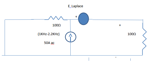
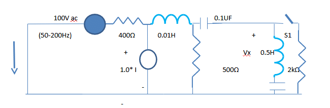
Table III. Frequency description of switch operation (Fig: 3)
| **** 10/14/23 16:46:40 ****** PSpice Lite (October 2012) ****** ID# 10813 **** |
| Frequency-dependent switch simulation |
| Circuit description |
| Voltage AC excitation |
| I 0 3 AC 1 |
| R13 0 3 100 |
| E34 3 4 LAPLACE {I(E34)} = {(ABS(S)/(2.0*3.141592653589793)-1700)*1E8} |
| R40 4 0 100 |
| .AC LIN 13 1KHz 2.2KHz |
| .PRINT AC VM(3) VP(3) VM(4) VP(4) |
| .OP |
| .end |
| **** 10/14/23 16:46:40 ****** PSpice Lite (October 2012) ****** ID# 10813 **** |
| Frequency-dependent switch simulation |
| Small signal bias solution Temperature = 27.000 DEG C |
| Node voltage |
| ( 3) 0.0000 ( 4) 0.0000 |
| Voltage source currents |
| Name Current |
| Total power dissipation 0.00E+00 watts |
| **** 10/14/23 16:46:40 ****** PSpice Lite (October 2012) ****** ID# 10813 **** |
| Frequency-dependent switch simulation |
| Operating point information Temperature = 27.000 DEG C |
| Voltage-controlled voltage sources |
| Name E34 |
| V-source 0.000E+00 |
| I-source 0.000E+00 |
| **** 10/14/23 16:46:40 ****** PSpice Lite (October 2012) ****** ID# 10813 **** |
| Frequency-dependent switch simulation |
| AC analysis Temperature = 27.000 DEG C |
| FREQ VM(3) VP(3) VM(4) VP(4) |
| 1.000E+03 1.000E+02 0.000E+00 1.429E-07 1.800E+02 |
| 1.100E+03 1.000E+02 0.000E+00 1.667E-07 1.800E+02 |
| 1.200E+03 1.000E+02 0.000E+00 2.000E-07 1.800E+02 |
| 1.300E+03 1.000E+02 0.000E+00 2.500E-07 1.800E+02 |
| 1.400E+03 1.000E+02 0.000E+00 3.333E-07 1.800E+02 |
| 1.500E+03 1.000E+02 0.000E+00 5.000E-07 1.800E+02 |
| 1.600E+03 1.000E+02 0.000E+00 1.000E-06 1.800E+02 |
| 1.700E+03 5.007E+01 0.000E+00 4.993E+01 0.000E+00 |
| 1.800E+03 1.000E+02 0.000E+00 1.000E-06 0.000E+00 |
| 1.900E+03 1.000E+02 0.000E+00 5.000E-07 0.000E+00 |
| 2.000E+03 1.000E+02 0.000E+00 3.333E-07 0.000E+00 |
| 2.100E+03 1.000E+02 0.000E+00 2.500E-07 0.000E+00 |
| 2.200E+03 1.000E+02 0.000E+00 2.000E-07 0.000E+00 |
| Job concluded |
The switch in Fig: 3 becomes active at 1700Hz as shown in Table III, and the voltage at node (3) becomes equal to node (4).
Table IV. Frequency description of switch operation (Fig: 4)
| **** 10/15/23 12:27:19 ****** PSpice Lite (October 2012) ****** ID# 10813 **** Frequency-dependent AC switch simulation |
| Circuit description |
| V2 1 0 AC 100 |
| R13 1 2 400 |
| HG1 2 0 V2 1 |
| L23 2 3 0.01 |
| R30 3 0 500 |
| C34 3 4 0.1UF |
| L46 4 6 0.5 |
| C60 6 0 0.1 |
| E45 4 5 LAPLACE {I(E45)} = {(ABS(S)/(2.0*3.14159265359)-150)*1E10} |
| R40 5 0 2000 |
| .AC LIN 4 50 200 |
| .PRINT AC VM(1) VM(3) VM(4) VM(5) |
| .OP |
| .end |
| **** 10/15/23 12:27:19 ****** PSpice Lite (October 2012) ****** ID# 10813 **** |
| Frequency-dependent AC switch simulation |
| Small signal bias solution Temperature = 27.000 DEG C |
| Node voltage |
| ( 1) 0.0000 ( 2) 0.0000 ( 3) 0.0000 ( 4) 0.0000 |
| ( 5) 0.0000 ( 6) 0.0000 |
| Voltage source currents |
| Name Current |
| V2 0.000E+00 |
| Total power dissipation 0.00E+00 watts |
| **** 10/15/23 12:27:19 ****** PSpice Lite (October 2012) ****** ID# 10813 **** |
| Frequency-dependent AC switch simulation |
| Operating point information Temperature = 27.000 DEG C |
| Voltage-controlled voltage sources |
| Name E45 |
| V-source 0.000E+00 |
| I-source 0.000E+00 |
| Current-controlled voltage sources |
| Name HG1 |
| V-source 0.000E+00 |
| I-source 0.000E+00 |
| **** 10/15/23 12:27:19 ****** PSpice Lite (October 2012) ****** ID# 10813 **** |
| Frequency-dependent AC switch simulation |
| AC analysis Temperature =27.000 DEG C |
| FREQ VM(1) VM(3) VM(4) VM(5) |
| 5.000E+01 1.000E+02 2.506E-01 1.243E-03 2.486E-12 |
| 1.000E+02 1.000E+02 2.507E-01 5.048E-03 2.019E-11 |
| 1.500E+02 1.000E+02 2.508E-01 1.132E-02 1.131E-02 |
| 2.000E+02 1.000E+02 2.510E-01 2.151E-02 8.606E-11 |
| Job concluded |
Table IV shows that at 150Hz, the switch is on, and the voltage at node (4) is transferred to node (5).
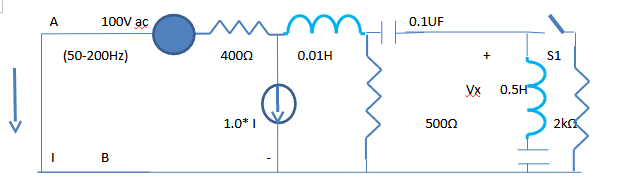
Fig: 5 shows an AC power circuit with a current controlled current source. Table V shows the netlist for the switch description and operation of Fig: 5. The switch is described with the symbol S1.
Table V. Frequency description of switch operation (Fig: 5)
| **** 10/15/23 19:35:45 ****** PSpice Lite (October 2012) ****** ID# 10813 **** |
| Frequency-dependent AC switch simulation |
| Circuit description |
| V2 1 0 AC 100 |
| R13 1 2 400 |
| FG1 2 0 V2 1 |
| L23 2 3 0.01 |
| R30 3 0 500 |
| C34 3 4 0.1UF |
| L46 4 6 0.5 |
| C60 6 0 0.1 |
| E45 4 5 LAPLACE {I(E45)} = {(ABS(S)/(2.0*3.14159265359)-150)*1E10} |
| R40 5 0 2000 |
| .AC LIN 4 50 200 |
| .PRINT AC VM(1) VM(3) VM(4) VM(5) |
| .OP |
| .end |
| **** 10/15/23 19:35:45 ****** PSpice Lite (October 2012) ****** ID# 10813 **** |
| Frequency-dependent AC switch simulation |
| Small signal bias solution Temperature = 27.000 DEG C |
| Node voltage |
| ( 1) 0.0000 ( 2) 0.0000 ( 3) 0.0000 ( 4) 0.0000 |
| ( 5) 0.0000 ( 6) 0.0000 |
| Voltage source currents |
| Name Current |
| V2 0.000E+00 |
| Total power dissipation 0.00E+00 watts |
| **** 10/15/23 19:35:45 ****** PSpice Lite (October 2012) ****** ID# 10813 **** |
| Frequency-dependent AC switch simulation |
| Operating Point Information Temperature = 27.000 DEG C |
| Voltage-controlled voltage sources |
| Name E45 |
| V-source 0.000E+00 |
| I-source 0.000E+00 |
| Current-controlled current sources |
| Name FG1 |
| I-source 0.000E+00 |
| **** 10/15/23 19:35:45 ****** PSpice Lite (October 2012) ****** ID# 10813 **** |
| Frequency-dependent AC switch simulation |
| AC analysis Temperature =27.000 DEG C |
| FREQ VM(1) VM(3) VM(4) VM(5) |
| 5.000E+01 1.000E+02 7.143E+01 3.542E-01 7.083E-10 |
| 1.000E+02 1.000E+02 7.144E+01 1.438E+00 5.754E-09 |
| 1.500E+02 1.000E+02 7.144E+01 3.224E+00 3.220E+00 |
| 2.000E+02 1.000E+02 7.147E+01 6.126E+00 2.451E-08 |
| Job concluded |
| **** 10/15/23 19:35:45 ****** PSpice Lite (October 2012) ****** ID# 10813 **** |
| Frequency-dependent AC switch simulation |
| Job statistics summary |
Switching recruitment for frequency-dependent systems varies depending on the application. There are different means by which switch performance can be evaluated and compared. These switches could be used at the design stage for different frequency ranges and power levels.
A frequency-dependent switch configuration is designed to fit in the PSpice simulation program for use in an electronic circuit (1700Hz,150Hz). The switch is tested and verified with four types of AC circuits in the frequency domain with the PSpice simulation software. Engineers with simulation experience can implement these conceptual designs and meet today’s advanced systems.
Author: K. Bharath Kumar, Researcher
The author obtained a B. Tech degree in E and CE with highest honours from JNT University, Anantapur, India, in 1981and M. Tech degree from Indian Institute of Technology, Kharagpur, India, in Microwave and Optical Communication in the year 1983. Later, he joined Indian Telephone Industries, Bengaluru, India and worked in Fiber optics. In 1990, he obtained an M.S. degree in electrical engineering from the Illinois Institute of Technology, Chicago, USA and joined Oki Electric, Japan, as a researcher in the semiconductor laboratory. He has over thirty-four publications in simulation and modelling of electronic circuits in various national and international journals. He is retired from Oki Electric now.

![[3 Pack] Sport Bands Compatible with Fitbit Charge 5 Bands Women Men, Adjustable Soft Silicone Charge 5 Wristband Strap for Fitbit Charge 5, Large](https://m.media-amazon.com/images/I/61Tqj4Sz2rL._AC_SL1500_.jpg)