
Check out our latest products

![[5G & 2.4G] Indoor/Outdoor Security Camera for Home, Baby/Elder/Dog/Pet Camera with Phone App, Wi-Fi Camera w/Spotlight, Color Night Vision, 2-Way Audio, 24/7, SD/Cloud Storage, Work w/Alexa, 2Pack](https://m.media-amazon.com/images/I/71gzKbvCrrL._AC_SL1500_.jpg)


A new method makes it possible to combine 2D materials with insulators—opening the door to smaller, faster electronics. Read more!
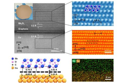
A team from Peking University, the Beijing Graphene Institute, and other Chinese institutions has introduced a new method to integrate 2D semiconductors with dielectric materials—insulators that regulate electric charge in devices. Their technique involves growing an ultra-thin dielectric film on a copper surface covered with graphene. This setup allows the film to be transferred to different substrates with minimal defects.
To demonstrate their new wafer-scale process, Lin and his team first synthesized a single-crystal dielectric called antimony oxide (Sb₂O₃). They then deposited this dielectric onto graphene grown on a Cu(111) substrate.

The process begins with the epitaxial growth of an Sb₂O₃ film on graphene using vacuum thermal evaporation. The copper substrate is pre-treated with a water-ethanol mixture to create a thin oxide layer, which reduces adhesion between the graphene and copper. The dielectric layer serves both as a support during transfer and as an encapsulating layer, protecting the structure from contamination and mechanical damage.
The researchers demonstrated that their process could reliably transfer a 4-inch graphene wafer onto target substrates with minimal defects. This achievement could pave the way for new electronic devices that combine 2D semiconductors with dielectric materials.
The method allowed the transfer of a 4-inch graphene wafer while preserving its intrinsic electrical properties, including an average carrier mobility of around 14,000 cm²/V·s. The integration with single-crystal dielectric Sb₂O₃ resulted in devices with excellent uniformity and long-term stability, showing minimal performance changes even after extended exposure to air.
This work holds strong practical potential, as the developed method could support the scalable production of high-performance, low-power microelectronics and optoelectronics based on 2D materials.
Future efforts will focus on advancing the transfer technique to enable stacking and precise alignment of 2D materials in three-dimensional configurations. This includes addressing key challenges such as interlayer coupling, interface control, and patterning, with the goal of building dense, high-performance electronic and optoelectronic systems.
Reference: Junhao Liao et al, Dielectric-assisted transfer using single-crystal antimony oxide for two-dimensional material devices, Nature Electronics (2025). DOI: 10.1038/s41928-025-01353-x.

![[3 Pack] Sport Bands Compatible with Fitbit Charge 5 Bands Women Men, Adjustable Soft Silicone Charge 5 Wristband Strap for Fitbit Charge 5, Large](https://m.media-amazon.com/images/I/61Tqj4Sz2rL._AC_SL1500_.jpg)