Check out our latest products
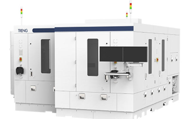
Featuring ±0.8μm accuracy and advanced thermal compression bonding (TCB), thesystem supports both large panels and glass substrates, overcoming traditional wafer limitations.

Toray Engineering Co., Ltd.has developed the UC5000, a high-precision semiconductor packaging system for panel-level packaging (PLP), an advanced technology experiencing growing demand, particularly for AI server applications. Sales will begin in April 2025. The UC5000 achieves chip packaging accuracy of ±0.8μm using thermal compression bonding (TCB) on large panels (515mm × 510mm and 600mm × 600mm) compliant with SEMI Standards. It is also capable of high-accuracy TCB packaging on glass panels, an emerging alternative to silicon, supporting next-generation semiconductor packaging.
The company aims to supply the UC5000 to semiconductor manufacturers, targeting 3 billion yen in orders for FY2025 and 10 billion yen by FY2030.As semiconductor performance advances, chiplet technology—integrating multiple chips into a single package—is gaining traction. Traditionally, wafer-level packaging using silicon wafers, such as interposers for high-speed transmission, has been standard. However, as chip packages increase in size, PLP on glass panels is attracting attention due to its larger, more efficient rectangular format, overcoming wafer size limitations.

Key innovations include:
- A proven TCB technology for small substrates, with over 100 mass-produced units, ensuring stable packaging even under high temperatures exceeding 300°C.
- High-accuracy packaging and warp-correction transfer technology, with at least 50 mass-produced units for large-panel systems.
- A newly redesigned core control system optimized for the UC5000.
Glass panels, however, present challenges such as significant warping, difficulty in transfer, and larger heating requirements. Maintaining heat control and achieving high-accuracy packaging while managing material expansion and contraction have been critical issues.It addresses these challenges with precision packaging technology refined from the company’s mass production experience.
Additionally, it supports front-opening unified pods (FOUPs) and tape frames meeting SEMI Standards, facilitating seamless integration into advanced semiconductor manufacturing processes.For more information, click here.


![[5G & 2.4G] Indoor/Outdoor Security Camera for Home, Baby/Elder/Dog/Pet Camera with Phone App, Wi-Fi Camera w/Spotlight, Color Night Vision, 2-Way Audio, 24/7, SD/Cloud Storage, Work w/Alexa, 2Pack](https://m.media-amazon.com/images/I/71gzKbvCrrL._AC_SL1500_.jpg)


![[3 Pack] Sport Bands Compatible with Fitbit Charge 5 Bands Women Men, Adjustable Soft Silicone Charge 5 Wristband Strap for Fitbit Charge 5, Large](https://m.media-amazon.com/images/I/61Tqj4Sz2rL._AC_SL1500_.jpg)


