Optimising Voltage Stability In Circuits With Simulation Tools And The Superposition Theorem

Check out our latest products

![[5G & 2.4G] Indoor/Outdoor Security Camera for Home, Baby/Elder/Dog/Pet Camera with Phone App, Wi-Fi Camera w/Spotlight, Color Night Vision, 2-Way Audio, 24/7, SD/Cloud Storage, Work w/Alexa, 2Pack](https://m.media-amazon.com/images/I/71gzKbvCrrL._AC_SL1500_.jpg)


In GPS and wireless communication, a constant voltage is vital at a desired network branch. But how to achieve that? One can take a circuit, for instance. Simulation tools like PSpice adjust network sections, while the Superposition Theorem and feedback sources restore the original values in the circuit.
Radio frequency (RF) circuits, commonly used in GPS and wireless communication systems, are designed using sinusoidal signals in both the time and frequency domains. These circuits rely heavily on established network and circuit principles.
Circuit simulation and analysis software, often called simulators, are essential tools for electronic circuit designers. These tools typically include functions like schematic capture, printed circuit board (PCB) layout, and bill of materials generation. Most simulators evolved from the SPICE (simulation program with integrated circuit emphasis) developed in the 1970s. They use techniques like Thevenin and Superposition theorems to analyse voltage and current at circuit nodes.
Initially, Spice operated in batch mode with text-based files describing circuits using netlist syntax. Over time, electronic design automation (EDA) companies added graphical interfaces for circuit building, improving simulation and visualisation. Popular early versions included PSpice and ElectronicsWorkbench (later Multisim). These tools evolved to support PCB layout creation, design rule checks, and BOM generation.
Simulation is also used in instrumentation, creating a ‘virtual lab bench.’ Some tools, like Fritzing, provide physical imagery of components, making simulations resemble real-world circuits. Circuit simulation software is available in both free and commercial versions, with free packages like SIMetrix offering limited features for educational use.

Networks and circuits
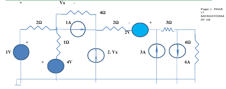
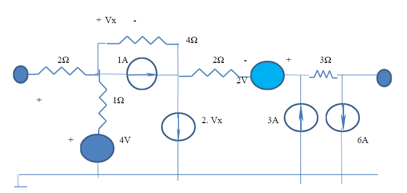
The Superposition theorem is widely used to obtain solutions to electronic and electrical networks using linear elements and small signal models for non-linear electronic and electrical devices. Circuit/network using electronic components and small signal device models is given (Fig.1). Several DC voltage and current sources are employed in these linear circuits.
Applying Superposition to DC semiconductor/MMIC networks
Fig. 1 shows the original circuit for which different individual networks to verify the Superposition theorem using SPICE/Pspice computer simulation have been written with software netlist. The node voltages and currents in the original circuit are obtained(verified) by an algebraic sum of individual nodes and currents.
Single-cell analysis and adjustment
The voltage source (4Volts) is (Figure 1) changed to (5V) and the value of the voltage and current across 6Ω is calculated using SPICE/PSpice software. The initial value across 6Ω is also evaluated with (4 volts). Two independent current sources (a) one across nodes (2-4) Ix and another (b) across nodes (7-0) Iy, are connected in the changed circuit so that their values can be adjusted to bring back the original voltage of the initial circuit.
To calculate the individual current source values Ix, Iy
First, the equation to obtain both Ix and Iy is obtained using the Superposition theorem for individual current sources connected across nodes (2-4)and (7-0). The individual trans-resistances for two current sources obtained by running Spice/Pspice software are ( RM1= -0.7742 Ω, RM2-=-2.51616666Ω ) respectively. The governing equation to obtain I and Iy is,
-10.2580-Ix. (0.77742)-Iy.(2.51616666)=-10.6450 ….. (1)
Choosing Ix=2A, Iy is (from (1)) -0.4615751475 A
The modified Spice/PSpice file to obtain the original voltage(-10.6450 Volts) across 6Ω resistor is given in Table I. The voltage values are verified with the original circuit.
Table I
| **** 07/17/23 14:11:59 ****** PSpice Lite (October 2012) ****** ID# 10813 **** |
| Superpositiontheorem circuit (problem 1) |
| **** Circuit description |
| *********************************************************************** |
| V10 1 0 DC 1 |
| R12 1 2 2 |
| R23 2 3 1 |
| V30 3 0 DC 5 |
| I24 2 4 DC 1 |
| II24 2 4 DC 2 |
| R24 2 4 4 |
| G40 4 0 2 4 2 |
| R45 4 5 2 |
| V65 6 5 DC 2 |
| IO6 0 6 DC 3 |
| R67 6 7 3 |
| I70 7 0 DC 6 |
| II70 7 0 DC -0.4615751475 |
| R70 7 0 6 |
| .END |
| **** 07/17/23 14:11:59 ****** PSpice Lite (October 2012) ****** ID# 10813 **** |
| Superposition theorem circuit (problem 1) |
| **** Small signal bias solution Temperature= 27.000 DEG C |
| *********************************************************************** |
| Nodevoltage |
| ( 1) 1.0000 ( 2) 1.4537 ( 3) 5.0000 ( 4) .1762 |
| ( 5) -1.3523 ( 6) .6477 ( 7) -10.6450 |
| Voltage source currents |
| Name Current |
| V10 2.269E-01 |
| V30 -3.546E+00 |
| V65 -7.642E-01 |
| Total power dissipation 1.90E+01 watts |
| Job Concluded |
Cascaded DC semiconductor network solution
Definition of the problem
The output voltage/current of the network should be controlled by the automatic voltage/current-dependent source according to the variation desired.
The individual contributions due to each energy source (current/voltage) should also be adjustable by a single independent source(s). Three similar circuits whose internal components/elements are described by Fig. 3 are cascaded as shown in Fig. 2a, and b describes the cascaded network in which independent sources in the second(2T) and third subnetwork (3T) are varied.
A solution to the problem with feedback
Using the Superposition theorem, individual contributions due to each varied/adjusted energy source are determined at the 1KΩ resistor at the output for each circuit. Using dependent current/voltage controlled voltage/current polynomial sources (feedback principle) and connecting them intelligently at the unvaried energy source at the first stage, we would get the original circuit in addition to varied circuits.
The following network (Fig. 3) is used in 2T, and 3T( two port boxes) in the cascaded networks described in Fig. 2a and b.

Table II
| **** 08/13/23 10:19:13 ****** PSpice Lite (October 2012) ****** ID# 10813 **** |
| Three cascaded identical circuits |
| **** Circuit description |
| *********************************************************************** |
| .SUBCKT CAS 1 3 5 6 7 |
| R12 1 2 2 |
| R23 2 3 1 |
| I24 2 4 DC 1 |
| R24 2 4 4 |
| G40 4 0 2 4 2 |
| R45 4 5 2 |
| IO6 0 6 DC 3 |
| R67 6 7 3 |
| .ENDS |
| X1 1 3 5 6 7 CAS |
| V30 3 0 DC 4 |
| V56 5 16 DC -2 |
| V166 16 6 DC 17.311827 |
| I70 7 0 DC 2 |
| V10 1 0 DC 10 |
| X2 7 8 9 10 11 CAS |
| V80 8 0 DC 4 |
| V910 9 10 DC -2 |
| I110 11 0 DC 6 |
| X3 11 12 13 14 15 CAS |
| V120 12 0 DC 4 |
| V1314 13 14 DC -2 |
| I150 15 0 DC 6 |
| R150 15 0 1K |
| .END |
| **** 08/13/23 10:19:13 ****** PSpice Lite (October 2012) ****** ID# 10813 **** |
| Three cascaded identical circuits |
| **** Small signal bias solution Temperature = 27.000 DEG |
| *********************************************************************** |
| Node voltage |
| ( 1) 10.0000 ( 3) 4.0000 ( 5) 9.2982 ( 6) -6.0136 |
| ( 7) -4.5927 ( 8) 4.0000 ( 9) .0716 ( 10) 2.0716 |
| ( 11) -6.3228 ( 12) 4.0000 ( 13) -4.7467 ( 14) -2.7467 |
| ( 15) -20.6850 ( 16) 11.2980 ( X1.2) 4.9073 ( X1.4) 2.3509 |
| ( X2.2) .3547 ( X2.4) -.3321 ( X3.2) .0809 ( X3.4) 1.2119 |
| Voltage source currents |
| Name Current |
| V30 9.073E-01 |
| V56 -3.474E+00 |
| V166 -3.474E+00 |
| V10 -2.546E+00 |
| V80 -3.645E+00 |
| V910 -2.019E-01 |
| V120 -3.919E+00 |
| V1314 2.979E+00 |
| Total power dissipation 1.11E+02 watts |
| Job Concluded |
| **** 08/13/23 10:19:13 ****** PSpice Lite (October 2012) ****** ID# 10813 **** |
Table III
| **** 08/13/23 12:38:23 ****** PSpice Lite (October 2012) ****** ID# 10813 **** |
| Three cascaded identical circuits |
| **** Circuit description |
| *********************************************************************** |
| *The DC currents(6A) in the II and III stage have been changed |
| * to 2A each |
| .SUBCKT CAS 1 3 5 6 7 |
| R12 1 2 2 |
| R23 2 3 1 |
| I24 2 4 DC 1 |
| R24 2 4 4 |
| G40 4 0 2 4 2 |
| R45 4 5 2 |
| IO6 0 6 DC 3 |
| R67 6 7 3 |
| .ENDS |
| X1 1 3 5 6 7 CAS |
| V30 3 0 DC 4 |
| V56 5 6 DC -2 |
| I70 7 0 DC 6 |
| V10 1 0 DC 10 |
| X2 7 8 9 10 11 CAS |
| V80 8 0 DC 4 |
| V910 9 10 DC -2 |
| I110 11 0 DC 2 |
| X3 11 12 13 14 15 CAS |
| V120 12 0 DC 4 |
| V1314 13 14 DC -2 |
| I150 15 0 DC 2 |
| R150 15 0 1K |
| .END |
| **** 08/13/23 12:38:23 ****** PSpice Lite (October 2012) ****** ID# 10813 **** |
| Three cascaded identical circuits |
| **** Small signal bias solution Temperature = 27.000 DEG C |
| *********************************************************************** |
| Node voltage |
| ( 1) 10.0000 ( 3) 4.0000 ( 5) 3.9281 ( 6) 5.9281 |
| ( 7) -4.7336 ( 8) 4.0000 ( 9) 2.1116 ( 10) 4.1116 |
| ( 11) .4129 ( 12) 4.0000 ( 13) 2.8059 ( 14) 4.8059 |
| ( 15) -1.1906 ( X1.2) 5.2908 ( X1.4) 5.0359 ( X2.2) .1586 |
| ( X2.4) -1.4226 ( X3.2) 1.9470 ( X3.4) .8035 |
| Voltage source currents |
| Name Current |
| V30 1.291E+00 |
| V56 5.539E-01 |
| V10 -2.355E+00 |
| V80 -3.841E+00 |
| V910 -1.767E+00 |
| V120 -2.053E+00 |
| V1314 -1.001E+00 |
| Total power dissipation 3.75E+01 watts |
| Job concluded |
Table I shows the Pspice netlist to calculate the output voltage across a one kilo-ohm load. Table III gives the output voltage across one kilo-ohm for changes in current sources in the second and third stages.
An additional voltage in series to the independent voltage source V30 is to be added at the first stage so that the output voltage from changed (-1.1906V) is brought back to the original unaltered (-20.6850V) at node (15) with altered values of changed dependent current sources (I110, I150).
The following circuit equations calculate the voltage that should be added to V30 at the first stage.
-1.1905568 + (0.0124)*V30DX= -20.6850
From which, V30DX= -1572.1290 volts
The changed voltage due to changes in independent current sources in the second and third stages, at the output node(15) is brought back to -20.6850, which is the original DC value at the output node(15) without any changes in all three cascaded stages (Table II), by applying corrected voltage. Table IV shows the Pspice netlist and results for obtaining (regaining) the original voltage across one kilo-ohm by adding V30DX.
Table IV
| **** 08/13/23 18:35:22 ****** PSpice Lite (October 2012) ****** ID# 10813 **** |
| Three cascaded identical circuits |
| **** Circuit description |
| *********************************************************************** |
| .SUBCKT CAS 1 3 5 6 7 |
| R12 1 2 2 |
| R23 2 3 1 |
| I24 2 4 DC 1 |
| R24 2 4 4 |
| G40 4 0 2 4 2 |
| R45 4 5 2 |
| IO6 0 6 DC 3 |
| R67 6 7 3 |
| .ENDS |
| X1 1 3 5 6 7 CAS |
| V30 3 16 DC 4. |
| EV160 16 0 VALUE= {(-20.6850+1.1905568)/(0.01239109784)} |
| V56 5 6 DC -2 |
| I70 7 0 DC 6 |
| V10 1 0 DC 10 |
| X2 7 8 9 10 11 CAS |
| V80 8 0 DC 4 |
| V910 9 10 DC -2 |
| I110 11 0 DC 2 |
| X3 11 12 13 14 15 CAS |
| V120 12 0 DC 4 |
| V1314 13 14 DC -2 |
| I150 15 0 DC 2 |
| R150 15 0 1K |
| .END |
| **** 08/13/23 18:35:22 ****** PSpice Lite (October 2012) ****** ID# 10813 **** |
| Three cascaded identical circuits |
| **** Small signal bias solution Temperature = 27.000 DEG C |
| *********************************************************************** |
| Node voltage |
| ( 1) 10.0000 ( 3)-1569.3000 ( 5) -854.7200 ( 6) -852.7200 |
| ( 7) -435.4600 ( 8) 4.0000 ( 9) -115.3600 ( 10) -113.3600 |
| ( 11) -58.3240 ( 12) 4.0000 ( 13) -16.7470 ( 14) -14.7470 |
| ( 15) -20.6850 ( 16)-1573.3000 ( X1.2)-1057.1000 ( X1.4)-1138.9000 |
| ( X2.2) -145.2800 ( X2.4) -158.0500 ( X3.2) -17.6340 ( X3.4) -18.7880 |
| Voltage source currents |
| Name Current |
| V30 5.121E+02 |
| V56 -1.421E+02 |
| V10 -5.336E+02 |
| V80 -1.493E+02 |
| V910 -2.135E+01 |
| V120 -2.163E+01 |
| V1314 -1.021E+00 |
| Total power dissipation 3.64E+03 watts |
| Job concluded |
Final thoughts
The SPICE/Pspice circuit simulation program makes modifications to individual sections of a cascaded network consisting of resistors and both dependent and independent energy or current sources. These adjustments are made to achieve the desired voltage or current at a specific branch of the circuit. The original voltages and currents in the target branch (with the energy sources unchanged) can be calculated by applying the Superposition theorem. The changes made to the cascaded network can then be compensated for using feedback polynomial sources, which are intelligently connected at the appropriate locations to restore the original voltages and currents in the circuit.
References
- K. Bharath Kumar, Norton Theorem Equivalent for Variable Circuit Element, Sources Using Spice/Pspice Circuit Simulations, Electro Bits Magazine, Issue:11. Volume 5, pp. 5-11, July 2023
- K. Bharath Kumar, Cascaded Transmission Parameters from Pspice Circuit Simulation, issue 8, Vol. 5, All About Electronics Magazine, pp. 51-58, June 2023
- K. Bharath Kumar, Methods to obtain a new circuit whose Thevenin and Norton Equivalents are functions of two different Thevenin and Norton Circuit, Electro Bits Magazine, pp. 37-44, May 2023
- Gorecki, K.(2008). SPICE Modeling and the Analysis of the Self-Excited Push-Pull DC-DC converter with Self-Heating Taken Into Account. Mixed Design of Integrated Circuits and Systems, MIXDES (6), pp. 19-21
- Izydorczyk, J., Chojcan, J.(2008).Tuning Of Coupled Resonator LC Filter Aided By SPICE Sensitivity Analysis. Computational Technologies in Electrical and Electronics Engineering, SIBIRCON (7), pp. 21-25
- Radwan, A. G., Madian, A. H., Soliman, A. M.(2016). Two-Port Two Impedances Fractional Order Oscillators. Microelectronics Journal,(9), pp. 40-52
- Steenput,E.(1999). A SPICE Circuit Can Be Synthesized With A Specific Set Of S-Parameters. IEEE PES Winter Meeting, January 31
- Yang, W. Y., and Lee, S. C.(2007) Circuit Systems with MATLAB and PSpice, Chapter X, State: John Wiley & Sons
- Rashid, M. H. (1995) SPICE for Circuits and Electronics Using PSPICE. Prentice Hall
- J. Keown, J.(2001). OrCAD PSpice and Circuit Analysis, Prentice Hall
- Du, H., Gorcea, D., So, P.P.M, Hoefer,W. J. R.(2008). A SPICE Analog Behavior Model Of Two-Port Devices With Arbitrary Port Impedances Based On The S- Parameters Extracted From Time-Domain Field Responses. International Journal of Numerical Modelling Electronic Networks, Devices and Fields, 21(1-2), pp. 77-90
- Xia, L., Bell,I. M., Wilkinson,A. J.(2011). Automated model conversion for analog simulation based on SPICE-level description. 6th International conference on Design & Technology of Integrated Systems in Nanoscale Era(DTIS), pp 1-4
- Roy, C. D., and Shail,B. J. Linear Integrated Circuits, New Age International Publisher, New Delhi
- Dillard, W. C.(2004). Is SPICE applicable across the ECE curriculum and proceedings. ASEE Southeast Section Conference
- Kumar, R. and Kumar, K.(2015). Pspice and Matlab/SimElectronic based teaching of Linear Integrated Circuit:A New Approach. International Journal of Electronics and Electrical Engineering, 3(2), pp. 34-37
- Lintao,L., Jinxiang, W., Mingyan, Y., Ming,J.(2008). A wide band circuit model of on-chip spiral inductor. International conference on Microwave and Millimeter Wave Technology, ICMMT,(6), pp. 375-377
- Smith,C. E.(1994). Frequency domain analysis of RF and microwave circuits using SPICE. IEEE Trans. MTT, 42( 10), pp. 1904-1909
- Neumayer,R. Haslinger,F. Stelzer,A., Weigel,R.(2002). Synthesis of SPICE compatible broadband electrical models from n-port scattering parameter data. IEEE International Symposium on Electromagnetic compatibility, 1(8), pp. 469-474
- Prigozy,S. (1989). Novel applications of SPICE in engineering education. IEEE Transactions on Education, 32( 1), pp. 35-38
- Nagel,L.W.(1975). SPICE 2, A Computer Program To Simulate Semiconductor Circuit. Electronic Research Laboratory Report ERL-M520, University of California, Berkeley
- SPICE version 2G user’s guide. (1975), University of California, Berkeley
- Wilson, B.(2007). Tutorial review trends in current conveyor and current mode amplifier design. International Journal of Electronics, 73(3), 533-583
- Bharath Kumar, K.(1990). Multi two port parameter simulation using Pspice, Technical Report, Semiconductor Research Laboratory, Oki Electric Industry, Japan
- C. C. Timmermann,C. C.(1995). Exact S Parameter models boost SPICE, IEEE Circuits & Devices Magazine,(9), pp, 17-22
- Kumar, K. B. and Wong, T. (1988). Methods to obtain Z,Y,G,H,S Parameters from SPICE program, IEEE Circuits and Devices Magazine, pages:30-31
By: K. Bharath Kumar, Researcher
The author obtained a B. Tech degree in E and CE with highest honours from JNT University, Anantapur, India, in 1981and M. Tech degree from Indian Institute of Technology, Kharagpur, India, around Microwave and Optical Communication in the year 1983. Later, he joined Indian Telephone Industries, Bengaluru, India and worked around Fiber optics. In 1990, I obtained an M.S. degree in electrical engineering from the Illinois Institute of Technology, Chicago, USA and joined Oki Electric, Japan, as a researcher in the semiconductor laboratory. He has over thirty-four publications on simulation and modelling of electronic circuits in various national and international journals. He is retired now.

![[3 Pack] Sport Bands Compatible with Fitbit Charge 5 Bands Women Men, Adjustable Soft Silicone Charge 5 Wristband Strap for Fitbit Charge 5, Large](https://m.media-amazon.com/images/I/61Tqj4Sz2rL._AC_SL1500_.jpg)