Check out our latest products
The design details GaN power devices, modular construction, and voltage sensing to optimize inverter performance. See more!
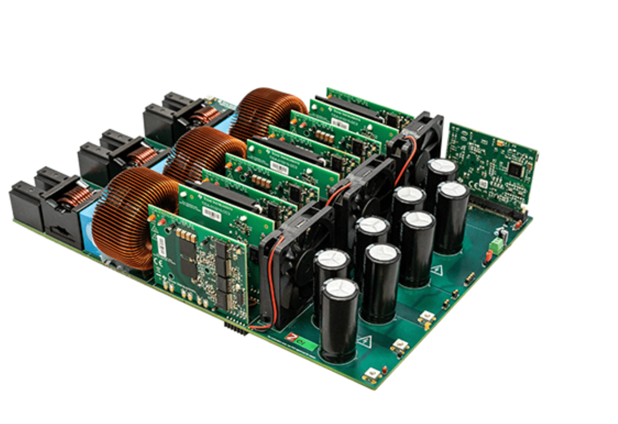
The solar inverter industry is experiencing advancements, leading to the development of smaller, efficient products. Innovations include the adoption of higher voltage solar arrays, the reduction in size of onboard magnetics, and the integration of localized power storage with bidirectional power stages. These improvements are enhancing performance and efficiency, with higher voltage arrays reducing current and conduction losses, while new inverter topologies and faster switching speeds enable more compact designs. For design engineers working on applications such as string inverters, DC wallbox chargers, and power conversion systems (PCS), the TIDA-010210 reference design from Texas Instruments offers a tool.
The fast-switching capabilities of GaN power devices enable operation at a higher frequency of 100 kHz, which reduces the size of the filter magnetics and enhances the power density of the power stage. The multilevel topology allows for the use of 600-V rated power devices, enabling higher DC bus voltages of up to 1000 V. The reduced switching voltage stress lowers switching losses, achieving a peak efficiency of 98.5%.

The modular construction of this reference design offers flexibility for engineers, allowing them to easily swap out power switching devices for direct comparisons between different configurations. The design consists of several key boards: a motherboard that includes the LCL filter, sensing electronics, bias power, switching relays, and cooling fans; a TMDSCNCD280049C Control Card that supports the DSP; and six power cards, each switching at 100 kHz with GaN power switching devices and isolated bias power supplies. Additionally, three power cards operate at 100 Hz and 120 Hz with Si power switching devices, gate drivers, and isolated bias power supplies.
Engineers can also take advantage of the design’s flexibility when it comes to power supply. While the reference design can accept 12-V bias power from an external supply, it also includes provisions for integrating an auxiliary power supply that can operate directly from the high-voltage DC bus, offering further versatility.

The reference design also incorporates voltage sensing at three points in the inverter signal path—before and after the primary output relay, as well as at the positive and negative bus voltages. This enables engineers to synchronize the control system with the grid voltage and frequency before connecting, preventing potential mismatch issues. Additionally, voltage sensing on the positive and negative bus voltages allows for fine-tuning of the duty cycle during both the positive and negative half cycles, ensuring precise operation and preventing bus voltage mismatches. This capability helps engineers optimize the inverter’s performance and achieve reliable, efficient operation in various applications.
TI has tested this reference design. It comes with a bill of materials (BOM), schematics, assembly drawing, printed circuit board (PCB) layout, and more. The company’s website has additional data about the reference design. To read more about this reference design, click here.


![[5G & 2.4G] Indoor/Outdoor Security Camera for Home, Baby/Elder/Dog/Pet Camera with Phone App, Wi-Fi Camera w/Spotlight, Color Night Vision, 2-Way Audio, 24/7, SD/Cloud Storage, Work w/Alexa, 2Pack](https://m.media-amazon.com/images/I/71gzKbvCrrL._AC_SL1500_.jpg)


![[3 Pack] Sport Bands Compatible with Fitbit Charge 5 Bands Women Men, Adjustable Soft Silicone Charge 5 Wristband Strap for Fitbit Charge 5, Large](https://m.media-amazon.com/images/I/61Tqj4Sz2rL._AC_SL1500_.jpg)


