
Check out our latest products

![[5G & 2.4G] Indoor/Outdoor Security Camera for Home, Baby/Elder/Dog/Pet Camera with Phone App, Wi-Fi Camera w/Spotlight, Color Night Vision, 2-Way Audio, 24/7, SD/Cloud Storage, Work w/Alexa, 2Pack](https://m.media-amazon.com/images/I/71gzKbvCrrL._AC_SL1500_.jpg)


The method uses vapor to make tin transistors that work and last, helping make low-cost, large-area electronics and better OLED screens.
Researchers at Pohang University of Science and Technology have developed a method to make TFTs using tin-halide perovskites. Their approach uses thermal evaporation along with lead chloride (PbCl₂) as a reaction starter.
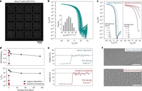
Based on these steps, a method was developed to fabricate tin perovskite TFTs. The strategy uses vapor deposition to deposit PbCl₂, tin iodide (SnI₂), and cesium iodide (CsI) onto a substrate.

In this method, the combination of these materials forms cesium-tin-iodide (CsSnI₃)-based perovskites, with PbCl₂ as the base layer. The chloride triggers solid-state reactions that convert the deposited precursors into perovskite films. This process also adjusts the hole density to levels suitable for use in transistor channel layers.
The resulting p-channel transistors showed performance with hole mobilities of 33.8 cm²/V·s and on/off current ratios around 10⁸. These values are similar to, and in some cases better than, those of devices made using solution-based methods. In contrast, earlier attempts at making perovskite transistors through deposition reported mobilities below 1 cm²/V·s, making them unfit for use. The vapor-deposited transistors also showed stability, which supports practical and scalable use.
Using this method, the researchers made and tested transistors, comparing them to transistors used in organic light-emitting diodes (OLEDs). Their devices outperformed IGZO-based oxide transistors used in OLED driving circuits.
The team believes that these p-type TFTs could help OLEDs work better and use less power. The study may also support more work on vapor deposition methods for making tin-halide perovskite transistors at scale. In time, this work could lead to large-area, low-cost VLSI electronics and stacked circuit designs.
Next steps include materials engineering and device integration. On the materials side, the goal is to explore compositions that allow lower-temperature processing and control over device traits such as turn-on voltage and hysteresis. On the application side, vapor deposition may allow vertical stacking of perovskite layers, leading to circuit designs without solvent-based photolithography. These directions could expand the use of perovskite-based electronics.
Reference: Youjin Reo et al, Vapour-deposited high-performance tin perovskite transistors, Nature Electronics (2025). DOI: 10.1038/s41928-025-01380-8.

![[3 Pack] Sport Bands Compatible with Fitbit Charge 5 Bands Women Men, Adjustable Soft Silicone Charge 5 Wristband Strap for Fitbit Charge 5, Large](https://m.media-amazon.com/images/I/61Tqj4Sz2rL._AC_SL1500_.jpg)